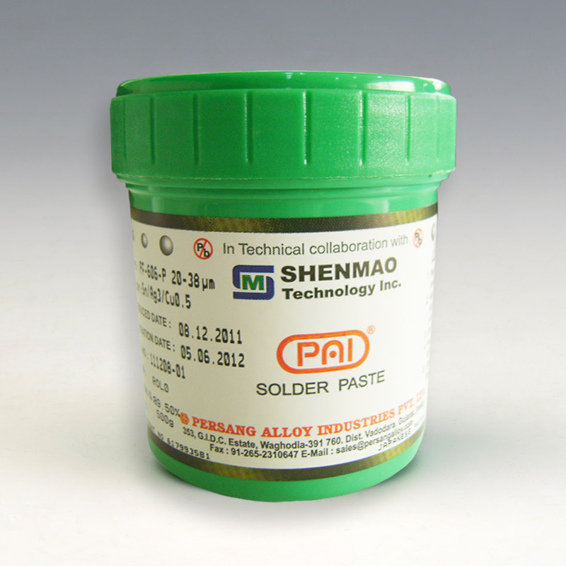
Description
–Specification—
| Item |
Specification |
Standard |
| Appearance |
Gray paste w/o visible foreign matter and clusters |
|
| Alloy composition |
Sn/Ag3.0/Cu0.5 |
JIS-Z-3282 |
| Melting Point |
217-219 °C |
|
| Particle Size |
(Type 3) +45μm < 1%, —20μm < 10%
(Type 4) +38μm < 1%, —20μm < 10% |
IPC-TM-650,2.2.14 |
| Powder Shape |
Spherical |
|
| Flux Content |
11 ± 1.0wt% |
JIS-Z-3197, 8.1.2 |
| Viscosity |
200 ± 30 Pa s (25±1 C°, 10rpm,Malcom ) |
JIS-Z-3284, Annex 6 |
| Flux Type |
ROL0 |
J-STD-004 |
—Test Content—
Test Item
|
Test Result
|
Test Method |
| Copper Plate Corrosion Test |
Pass |
JIS-Z-3197, 8.4.1 |
| Spread Test |
> 75% |
JIS-Z-3197, 8.3.1.1 |
| Copper Mirror Test |
Pass |
IPC-TM-650, 2.3.32 |
| Viscosity Test(25 °C,10rpm) |
200 ± 30 Pa • s |
JIS-Z-3284. Annex 6 |
| Tackiness Test (gf) |
> 140 up (8hr) |
JIS-Z-3284. Annex 9 |
| Slump Test |
Pass |
JIS-Z-3284. Annex 7, 8 |
| Solder Ball Test |
Pass |
JIS-Z-3284. Annex 11 |
—Reliability Test—
| S.I.R. Test ◊ |
> 1×10⁹ Ω , Pass |
IPC-TM-650, 2.6.3.3 |
| Electro Migration Test ♦ |
Pass |
IPC-TM-650, 2.6.14.1 |
◊ Test Conditions: 85 °C, 85% RH for 168 hrs ♦Test Conditions: 65 °C, 85% RH for 596 hrs
—Alloy Composition—
| (Sn) |
(Ag) |
(Cu) |
(Ni) |
(Ge) |
(Zn) |
(Al) |
(Sb) |
(Fe) |
(As) |
(Bi) |
(Cd) |
(Pb) |
| REM. |
2.8~3.2 |
0.3~0.7 |
0~0.01 |
0~0.01 |
0.001 MAX |
0.001 MAX |
0.05 MAX |
0.02 MAX |
0.03 MAX |
0.10 MAX |
0.002 MAX |
0.05 MAX |
Patent No. • Japanese Patent No. 3296289 • U.S Patent No. 6179935B1. Germany Patent No. 19816671C2 (Wt%)
—Temperature Profile—

| Ramp up rate(30~150 °C): |
1.0~2.0 °C/sec |
| Pre-heating time(155~185 °C): |
30~120 sec |
| Time period above 220 °C: |
30~100 sec |
| Ramp up rate during reflow: |
1.0~2.0 °C/sec |
| Peak temprature |
230~250 °C |
| Ramp down rate during cooling: |
1.0~6.0 °C/sec |
—Handling and Storage Instructions—
- 1. Storage
- (1) Refrigerate pastes at 0~10 °C to prolong shelf life; normal shelf life is 6 months from production date (sealed jars).
- (2) Keep away from direct sunlight.
- 2. Use (Sealed)
- (1) Allow pastes to reach ambient printing temperature prior to use for 3 – 4 hrs. Do not heat or raise temperature abruptly.
- (2) Mix paste well with plastic spatula for 1-3 mins before use. Mixing time depends on tool type.
- 3. Use (Opened)
- (1) At first, add 2/3 jar of solder paste onto the stencil. Do not add more than 1 jar.
- (2) Add a small amount of paste at a time on the stencil according to printing speed.
- (3) It is recommended to finish fresh paste within 24 hrs. To maintain paste quality, make sure not to store used paste and fresh paste in the same jar.
- (4) After printing, it is suggested to place components to be mounted on the circuit board and reflow within 4 – 6 hrs.
- (5) If printing process was interrupted for more than 1 hr, be sure to remove paste remnant from stencil and seal them in the jar.
- (6) It is recommended to keep printing environment at 22~28 °Cand RH of 30~60%.
- (7) To clean up printed circuit boards, it is suggested to use ethanol or isopropanol.